Author: Stefan Delleman
Short-wave listeners often are not able to, or allowed to, install a long-wire antenna or other large dimension antenna in or around the home.
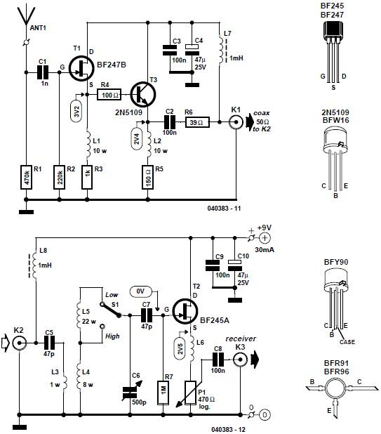
In such cases, the present active antenna, intended for the frequency range 3–30 MHz, may be found useful. The author used a 1-metre long rod or brass tube with a diameter of 2–6 mm. The circuit consists of two parts, one to be located close to the antenna, while the other should be placed in the associated power supply of the receiver.
The two sections may be connected by a coaxial cable of up to 20 m long without causing any discernible attenuation. The antenna signal is pre-amplified by a two-stage combination, T1-T3. The main amplification is provided by the input transformer, formed by L3, L4, and L5, in the receiver section. This is followed by a switch that enables the frequency range to be selected (3–10 MHz in position LOW, and 9–30 MHz in position HIGH). The signal strength may be adjusted to suit the receiver with potentiometer P1.
The active antenna is readily constructed with the aid of the two printed circuit boards shown.
Since we are concerned with only relatively low radio frequencies, the choice of components is not too crucial. Various types of FET may be used: BF245, BF246, BF256, or the SMD variants of these, but do mind their connections! The same applies for the transistors: BFW16, BFY90, BFR91, BFR96; any of these will do.
A few hints for readers who conduct their own experiments. A lower value of capacitor C1 results in a somewhat looser coupling to the antenna, but also in lower signal strength. It may be worthwhile to replace the capacitor with a variable type. Inductor L6 ensures that the output voltage at higher frequencies (30 MHz) is not much higher than at lower frequencies (3 MHz). This is because the Q factor of coils L4 and L5 increases at higher frequencies, which leads to higher amplitudes. This is compensated by L6. This inductor may be omitted and replaced by a wire bridge, but then the output voltages at higher frequencies increases.
 |
![404383uk[3] 404383uk[3]](https://blogger.googleusercontent.com/img/b/R29vZ2xl/AVvXsEgyjAMH5tZcsxEGiFSu_NfrVtBIYxRrNs8sxQyGwSWRFgpokwDRlve7sF5bHchIyjgJXidYlMv4pS2WbJoNM6k-Oudp74GDMtvUWyD1WPo3ZmzUG7hPUumJk0SjSgCorJviQS346EZDnifj/?imgmax=800) |
| PCB layout |
Aim at obtaining as tight a coupling as feasible between L4 and L5. Because of this, it is better to wind the two coils as one, that is, 30 turns with a tap than to wind two separate coils (see photograph).
COMPONENTS LIST
| Resistors | Inductors |
| Capacitors | Semiconductors Miscellaneous |
(Elektor Electronics Magazine – 07-08/2006)
 | Download this article (#040383-uk.pdf) |
Labels
- * Elektor 2005 (9)
- * Elektor 2006 (72)
- Adapters (1)
- ADC / DAC (1)
- AM / FM (2)
- Amplifiers (3)
- Antennae (2)
- Articles List (1)
- Audio (1)
- Automatic (2)
- Batteries (3)
- Bluetooth (1)
- Breakers / Contacts (1)
- Buzzers / Sirens (1)
- Clocks / Timers (2)
- Computer (2)
- Converters (2)
- Coolers / Fans (1)
- Counters (1)
- Datasheets (7)
- E-blocks (1)
- Energy (2)
- Flash / Light (8)
- Frequency (1)
- Fuse (1)
- Generators (2)
- High-voltage (1)
- Indicators (2)
- Infrared (IR) (4)
- LCDs (1)
- LEDs (7)
- Magazines (1)
- Meters (5)
- Microcontroller (9)
- Mobile Phone (1)
- Motors (1)
- OPAMP (3)
- PCB (1)
- Photosensors (1)
- Power Supply (2)
- Preamplifiers (1)
- Programming (3)
- Radio (1)
- Rectifiers (1)
- Regulators (1)
- Relays / Switches (10)
- Remote Control (7)
- RS232 (3)
- Security (4)
- Sensors (2)
- Servo (2)
- Simulators (1)
- Small Circuits (46)
- Telephones (2)
- TENS (1)
- Testers (3)
- Timebase (1)
- Tools (1)
- Transmitters (1)
- Trigger (1)
- USB (2)


0 comments: